ナノ構造分野 Nano Materials
清水教授 Prof. Shimizu
物質をナノスケールまで小さくしていくと、大きな材料(バルク)とは異なる性質を示すようになります。このナノ構造分野では特にナノワイヤやナノホールなど一次元ナノ構造体を「自己組織化」を利用して形成する方法を研究しています。我々はナノ構造形成を基盤技術として、次世代メモリ素子、3次元配線、バイオ・化学センサー、バイオミメティックス、太陽電池などへの研究展開を行っています。その意味で、ナノ構造分野は本研究室活動の根幹を支える部分です。これまでシリコン基板上での陽極酸化アルミナ・ナノホール形成法技術、単結晶シリコンナノワイヤの成長方位制御技術など、独創的なナノ・マイクロ構造体の形成方法を確立してきました。これらの技術は世界でも高く評価され、国際共同研究や企業との共同研究に発展してきました。現在では、これまでのナノワイヤやナノホール形成に加え、CuSnナノツリーや金属触媒を用いたシリコンのエッチング加工技術など新たな研究を行っています。
Nano-sized materials are known to have excellent properties such as band gap widening and magnetic properties by quantum confinement effect. We have studied fabrication of these nano materials such as one dimensional nanowires and nanoholes by “self-organization” processes. We developed these technologies for fabrication of next generation nonvolatile memories, 3-dimensional interconnections, biochemical sensors, bio-mimetics, and solar batteries, etc. Our original technologies are; (1) formation of nanohole array on Si using anodic oxidation of sputtered Al films, (2) growth of single crystalline Si nanowires perpendicular to Si (001) substrate, (3) CuSn nanotrees formed by electroplating, etc. These topics have been developed by collaboration between foreign research institutes and Japanese companies. Recently we have started metal assist chemical etching (MacEtch) of Si aiming at TSV and Si nanowire formation.
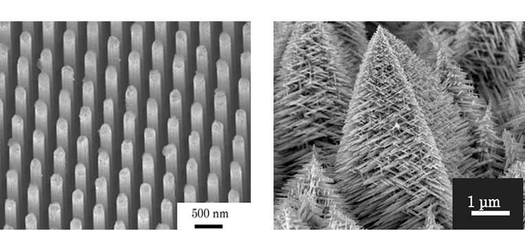
陽極酸化アルミナを用いたナノワイヤ配列構造の形成
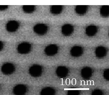
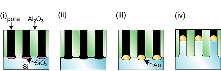
陽極酸化アルミナ(AAO)はアルミをアノード酸化すると得られる多孔質の被膜のことです。陽極酸化アルミナの孔(ナノホール)の直径は数nm~数百nmで、基板に対し垂直方向に配列成長します。このナノホールを鋳型として金属や半導体材料を埋め込み、細線材料(ナノワイヤ)を形成します。本研究室では様々な材料でのナノワイヤの形成や、ナノホールに埋め込んだ材料の結晶方位の制御に関する研究を行っています。参考文献![]()
AAO (anodic oxidation of aluminium) has been used by various researchers in the world. This is a simple technology uses pure aluminium film or plate with applying voltage in acidic solutions. It has been reported in the 1990s that the ordered array of nanoholes between a few tens to hundreds nm are formed perpendicular to substrate in oxalic acid, surfuric acid, and phousphoric acid. We deposited various materials such as metals and semiconductors by electroplating as well as electroless plating in the AAO nanoholes on Si o SiO2 substrate. These structures are very useful for biosensing devices as well as high density memories. Reference![]()
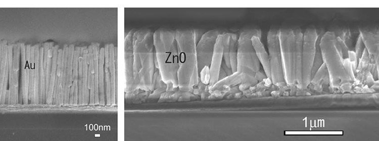
CuSnナノツリーの形成と成長メカニズムに関する研究
我々は銅と錫を特殊な条件下で同時にめっきすると、直径が数十ナノメートルスケールの枝を持つ樹枝状結晶が成長することを発見しました。この材料は各枝が高品質な単結晶であり、形状もユニークであることから、様々な用途への応用が検討されています。ナノ構造分野ではナノツリー材料の成長のメカニズムを調べ、異なる材料や形状の制御など用途に合わせたナノツリーの合成に役立てる研究をしています。 参考文献![]()
Formation of three-dimensional CuSn nanotree and investigation of its growth mechanism
We found that formation of nano-tree-like structures consisting of single crystal CuSn alloy nanowires branching perpendicularly from their parent branches. The nanotrees are being considered as various applications due to their unique structure and high-quality CuSn single crystal. We investigate a growth mechanism of the nanotree to contribute to control of the the intended shape of nanotree and to use other materials instead of Cu-Sn alloy. reference![]()
金属触媒を用いたシリコン基板の選択エッチング(メタルアシストエッチング)に関する研究
金や銀など貴金属を触媒として、フッ化水素酸などを含む溶液を用いるとシリコンを選択的にエッチングできます。我々はこの金属触媒の形やエッチング条件を工夫し、様々な形状のナノ・マイクロシリコン構造体を形成する研究を行っています。
Selective and high-aspect etching of semiconductor materials using metal-assisted chemical etching (MacEtch)
In MacEtch, Si is etched only at the interface of the Si and noble metal catalyst, which provides high selectivity and directionality for the etching of Si. Noble metals have been the dominant catalysts for MacEtch of Si substrate. We study about effects of the etching conditions for the formation of nano- micro-Si structure using MacEtch process.
バイオセンサー(ケミカルセンサー)分野 Biosensor
伊藤教授 Prof. Ito
バイオセンサーに関わる技術は、機械工学、応用物理学、電子工学、分子生物学、分析化学、電気化学など多岐にわたり、学部で学んできたこと以外にも多くの知識が必要となります。学内外の協力者と共に教員を含めて勉強をしつつ新しい分野への挑戦を行っています。また、IoTがクローズアップされる現代では、センサーの利用法などにも着目することが必要で、例えば一次産業に向けたセンサーなど時代のニーズに応えるセンサーの開発が望まれています。
私たちのグループでは、今までに培ってきたナノ・マイクロ領域の材料創製技術であるトップダウン法、ボトムアップ法を活用しながら新規ナノ材料を創製し、それらの物理的・化学的特性を明らかにしていきます。また、それら新規材料を用いたケミカルセンサを構築し、センサシステムへと展開することを行っています。
Molecular interaction such as PPI (protein-protein interaction) is very important for living organisms to maintain the life activity. In particular, PPIs are studied for drug discovery and basic medicine. For monitoring PPIs, many techniques are suggested based on photo fluorescence. However, this technique needs to label fluorescence materials. To monitor PPIs on the real time, some techniques such as SPR (surface plasmon resonance) and QCM (quartz crystal microbalance) are widely spread. These techniques have sensing devices, in fact, biosensors. Our group develops devices to monitor PPIs and complicated deformation of biomolecules using LSPR (Localized Surface Plasmon Resonance) and QCM. We develop these devices to improve the sensitivity by using nano structures which have large surface area.
バイオミメティクス分野 Biomimicry
伊藤教授 Prof. Ito
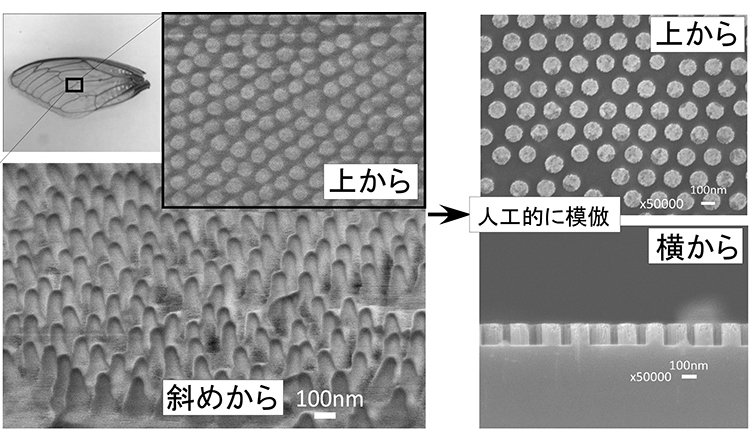
生物がその進化の過程で得てきたその生物特有の特徴的な機能がクローズアップされています。バイオミメティクスは、そのような生物が持つ特徴的な機能を真似ることで人類に役立つ技術を創出する研究分野であり、バイオミミクリーなどとも呼ばれています。私たちは、特に生物の持つナノ・マイクロ構造とその機能に着目しています。これらの構造は、自己組織化されており、低環境負荷で作られるため工業的に見ても有用です。
現在は、セミの羽の表面にあるナノ構造に着目し、そのナノ構造が持つ抗菌性について研究を行っています。ボトムアップ技術を使ってシリコン基板上に無数のナノ構造を作製することで模倣に成功しました。また、このナノ構造を表面に持つシリコン基板は、大腸菌に対して抗菌性を示すことを明らかにしてきました。今後は、これらの大量生産へ向けた取り組みにより食品分野などへ展開していきます。
Biomimetics is one of the hot topics in the world. Recently, observation techniques such as SEM, TEM and AFM are widely spread, and we can use them easily to discuss the nano and micro-structures of living organisms. They acquire functional nano and micro structures along the course of evolution. In addition, nano and micro fabrication techniques based on top down process and bottom up process grow up. Then, we can fabricate nano and micro-structures to mimic that of living organism.
We pay attention for cicada’s wing because it shows the antireflection, super hydrophobic, low friction and antibacterial property. In particular, antibacterial property is very unique and expressed due to physicochemical property of its structure. Our group fabricates Si nanopillars by metal assisted chemical etching and shows their antibacterial property. Now, we try to work out the mechanism of antibacterial property.
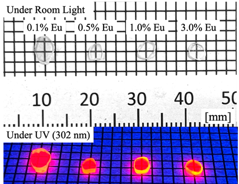
高エネルギー量子変換分野
市場助教 Asst. Prof. Ichiba
放射線計測は原子力関連施設の安全管理、核セキュリティ、非破壊検査、医療・産業利用などを支える重要な基盤技術であり、応用先に応じて様々な検出器が利用されています。中でも、固体検出器は検出効率の高さや取り扱いの容易さから広く用いられています。当該検出器は主に高エネルギーの放射線を紫外-可視-近赤外領域の光子に変換する蛍光体材料 (シンチレータやドシメータ材料)とそれらの光子を電気信号として出力する光検出器から構成されています。これら二つの構成要素のうち、シンチレータやドシメータ材料は、検出効率やエネルギー分解能といった検出器性能や応用先を決定づける重要な役割を担っています。それゆえ当グループでは放射線計測技術の更なる高度化を目指し、新しいシンチレータやドシメータ材料の創成に取り組んでいます。
Radiation measurement is a fundamental technology supporting safety management in nuclear-related facilities, nuclear security, non-destructive testing, and medical and industrial applications, and a variety of detectors are employed depending on the intended application. Among them, solid-state detectors are widely used because of their high detection efficiency and ease of handling. These detectors generally consist of phosphors, such as scintillators and dosimeter materials, which convert high-energy radiation into photons in the ultraviolet, visible, and near-infrared regions, and photodetectors that convert those photons into electrical signals. Of these two key components, scintillators and dosimetric materials play a crucial role in determining detector performance, including detection efficiency and energy resolution, as well as the range of possible applications. For this reason, our group is engaged in the creation of novel scintillator and dosimeteric materials with the aim of further advancing radiation measurement technology.